Electronics Tech Update – 11 April 2026

Semiconductor Expansion, AI Chip Manufacturing, and Electronics Industry Growth Trends

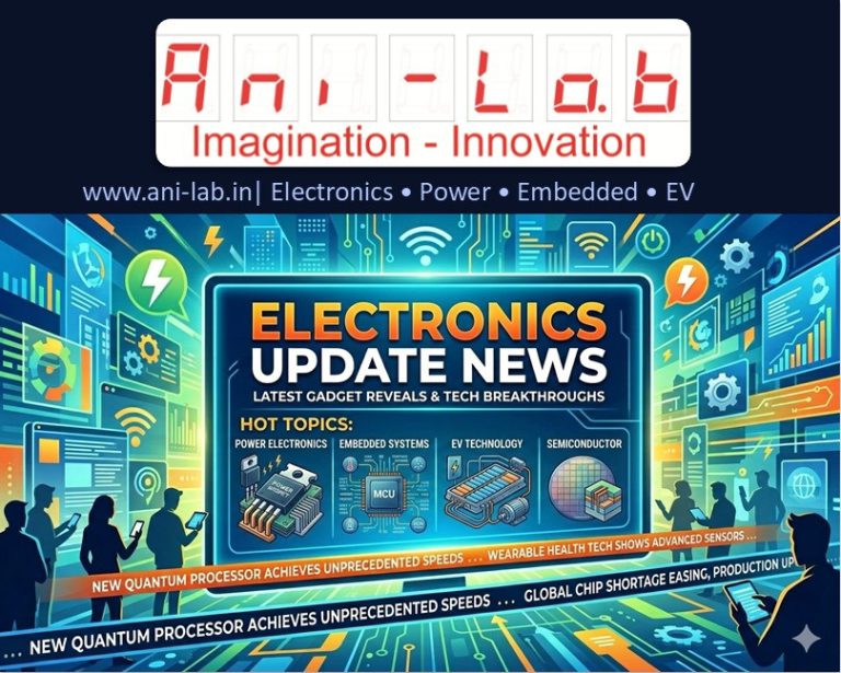
The global electronics and semiconductor industry continues to evolve rapidly with major investments in fabrication, packaging, and AI-driven chip development. Today’s update focuses on key developments that are directly relevant for electronics design engineers, especially those working in power electronics, embedded systems, and hardware design.


1. India Accelerates Semiconductor Ecosystem with New ATMP Facility

India has taken a major step toward becoming a global semiconductor hub with the launch of its first ATMP (Assembly, Testing, Marking, and Packaging) facility. This marks a critical shift from dependency on imports to localized backend semiconductor processing.

This initiative is part of the India Semiconductor Mission 2.0, which focuses not only on chip manufacturing but also on building a complete semiconductor ecosystem including packaging, materials, and design IP.

Key engineering implications:

  • ATMP facilities handle critical backend processes such as wire bonding, flip-chip packaging, and reliability testing
  • Packaging technology directly impacts thermal performance, EMI, and switching efficiency in power electronics
  • Local manufacturing reduces supply chain delays for ICs like controllers, MOSFET drivers, and DSPs

India has already approved 10 semiconductor projects, including fabrication and packaging units, with significant investment inflow.

For engineers, this means better availability of components like:

  • Digital controllers for SMPS (e.g., TI C2000 series)
  • Power ICs for PFC and LLC converters
  • Automotive-grade microcontrollers

2. Global Chip Demand Surges with 46% YoY Growth

The semiconductor market is experiencing massive growth driven by AI, EVs, and industrial automation.

According to the Semiconductor Industry Association, global chip sales reached $82.5 billion in January 2026, marking a 46.1% increase year-over-year.

Why this matters for design engineers:

  • Increased demand for power management ICs (PMICs)
  • Rapid adoption of wide bandgap devices (SiC, GaN)
  • Growth in high-frequency SMPS designs

This demand surge also explains why:

  • Component lead times fluctuate
  • Prices of power semiconductors remain volatile
  • Engineers must design with alternate part strategies

3. Tesla Announces “Terafab” AI Chip Manufacturing Project

In a major breakthrough, Tesla along with SpaceX has announced a next-generation semiconductor facility called Terafab.

Key highlights:

  • Target: 1 terawatt AI compute capacity per year
  • Technology node: 2 nm class process
  • Fully integrated facility (design → fabrication → packaging → testing)

Engineering significance:

  • Integration reduces parasitics and signal integrity issues
  • Enables faster iteration cycles in chip design
  • Focus on AI accelerators and high-performance computing chips

The project also aims to produce Tesla’s next-gen AI5 chip, expected to power autonomous systems and data centers.


4. Samsung Expanding Semiconductor Packaging Investments

Samsung Electronics is reportedly planning new investments in chip testing and packaging facilities in Vietnam.

This indicates a strong global shift toward advanced packaging technologies such as:

  • 2.5D / 3D IC packaging
  • Chiplet-based architectures
  • High-density interconnect substrates

Why this matters:

  • Packaging is now as critical as fabrication
  • Engineers must consider thermal resistance and parasitic inductance at package level
  • High-speed designs require co-design of PCB + package

5. India’s Electronics Production Target: $300 Billion by 2026

India’s electronics manufacturing sector is projected to reach $300 billion by 2026, driven by government incentives and global supply chain shifts.

Key opportunities for engineers:

  • Growth in consumer electronics SMPS design
  • Expansion of EV chargers and power electronics systems
  • Increased demand for embedded system developers

This also aligns with policies promoting:

  • Domestic PCB manufacturing
  • Component ecosystem development
  • Design-led manufacturing (not just assembly)

6. Supply Chain Constraints Continue in Advanced Nodes

Despite growth, challenges remain:

  • Advanced node fabrication (≤5 nm) is still constrained
  • Backend packaging bottlenecks affect availability
  • AI chip demand is outpacing production capacity

Recent reports highlight tightening supply in high-performance chips due to limited advanced manufacturing capacity.

For engineers, this means:

  • Design flexibility is critical
  • Avoid dependency on single IC vendors
  • Use modular and scalable architectures

Key Takeaways for Electronics Engineers

  • Semiconductor ecosystem is shifting toward local manufacturing and advanced packaging
  • AI is driving demand for high-performance and power-efficient chips
  • Packaging and thermal design are becoming as important as circuit design
  • Supply chain constraints require robust design strategies

About The Author

Aniruddh Kumar Sharma

I am an electronics enthusiast.

Articles: 255

Leave a Reply

Your email address will not be published. Required fields are marked *